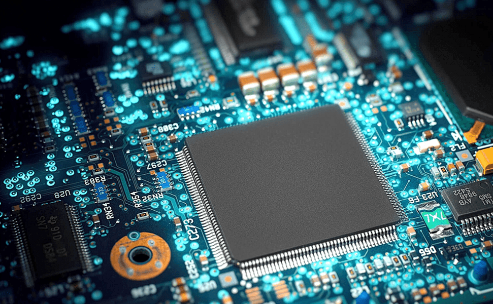
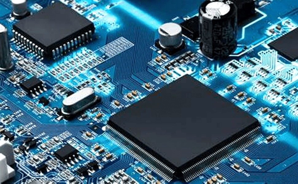
An embedded PCB has both the active and the passive components in its layers, making it compact compared to other normal PCBs.
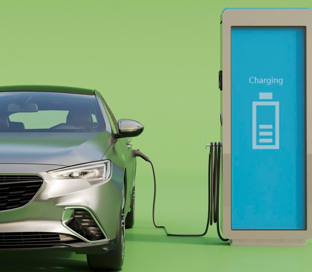
PCBs are widely used today because they enable the integration of complex circuits into a small area. They enhance overall performance and power consumption, which is beneficial in Smartphones, Medical devices, and Automotive applications.
Some recent practices in PCB prototyping include the use of high-frequency laminates, the use of automation and artificial intelligence in design, and the integration of 3D printing methods. These advancements provide a shorter time to market, enhanced accuracy, and the capacity to produce complex and versatile PCBs.
Table of Contents
ToggleEmbedded PCB: The Concept
Some of the features of embedded PCBs include placing resistors and capacitors on the board to minimize size and enhance performance. This integration helps to avoid some interface problems and allows for the design of more complicated and reliable electronics, so it confirms the feasibility of using the embedded PCB for high-end applications.
How is it different from Traditional PCB?
Embedded PCB is different from the traditional PCB because of the component stacking. In embedded PCB the resistors, transistors, and other components are placed inside the board’s layer. They also have some benefits, including helping minimize the size and amount of interference between signals.
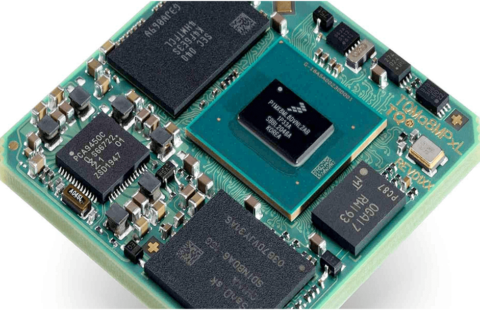
Some of the essential parts seen in the embedded PCB are embedded passives and actives, microcontrollers, and sensors. Due to their excellent electrical insulation and thermal stability, high-performance laminates and substrates such as FR4 and polyimide are usually used as the base material. They are used in constructing complex, strong, and efficient electronic items that are highly demanded in the market.
Applications of Embedded PCBs
Consumer Electronics
Embedded PCBs are commonly used in consumer electronics like smartphones and tablets to design compact solutions with high efficiency, which are indispensable for modern gadgets.
Medical Devices
In medical devices, embedded PCBs, including pacemakers and diagnostic apparatus, are essential in building effective and efficient products for the current medical sector. This way, they positively impact the lives of people with various conditions and their attendants.
Automotive Systems
Automotive systems depend on embedded PCBs to support various functionalities, such as self-driving cars, entertainment systems, and car safety, that assist in building smart and safe automobiles.
Initial Design Considerations
Defining the design goal is important because it defines the path of the entire prototyping process. A well-defined goal transforms the final product to meet the set functionality, performance, and cost objectives. It aids in avoiding costly mistakes and project delays since it offers a clear path for the design team to follow and guarantees that all the team’s efforts are directed toward meeting a single goal.
Gathering Requirements and Specifications
Identifying the detailed requirements and specifications is crucial to successfully developing a PCB design. These requirements identify the project’s requirements, the conditions in which it will be implemented, and the legal framework governing it.
In this case, clear and detailed requirements will guide the identification of the right components, materials, and design approaches to ensure that the PCB will work as required in its application and the prevailing environment.
Selecting the Right Materials and Components
When choosing the materials and components for an embedded PCB, it is important to consider durability, conductivity, and size. Long-lasting materials make products strong and reliable, good conductivity improves electrical efficiency, and correct dimensions provide for small and effective products. These factors are important for achieving maximum effectiveness and fulfilling the requirements of a particular application.
Innovations in PCB Materials
New standards in PCB materials are high-frequency laminates and flexible substrates. These high-frequency laminates have good electrical characteristics and low signal attenuation and are, therefore, suitable for high-speed uses. Flexible substrates increase design freedom and allow the development of more intricate and sophisticated electronics, which is crucial for most applications.
Design Software and Tools
Altium Designer, Eagle and KiCad are the most common and popular tools for designing the PCB. Eagle is also easy to use, with a nice user interface and many libraries for components. KiCad, being an open-source tool, provides a complete package with many users supporting it, thus making it cost-effective for many designers.
When choosing the tools, the following factors should be considered: collaboration, simulation, and a large number of components.
Collaboration allows workers to work on the design efficiently. Simulations can help create visuals and enhance the efficiency of the board. Using a large number of components is time efficient since it requires less time.
Rapid Prototyping Techniques
Creating a PCB sample quickly allows one to evaluate the design that was created through rapid prototyping. This technique uses processes such as 3D printing and CNC milling to produce samples of the designs quickly, enabling the designers to assess and modify the concepts used.
Benefits and Limitations
Time to market, cost, and flaw deduction are some of the benefits of rapid prototyping. However, some constraints can be listed, such as the fact that what is designed on the computer could be different from the final product due to different materials and less precise manufacturing methods.
However, rapid prototyping is still one of the most useful strategies for developing good PCBs.
Iterative Design and Testing
Iteration is important during the process of producing PCB prototypes because it allows the designers to keep modifying the design until the desired results are achieved.
Through testing and tweaking the prototype, the designers can eliminate problems and find solutions, ensuring that the final product is as expected and efficient.
Strategies for Efficient Testing and Validation
Some effective testing and validation methods include functional testing, where the embedded PCB is tested to real-time conditions, and automated testing, where special software checks for design faults.
Furthermore, environmental testing is used to determine whether the PCB can handle different conditions, such as temperature changes and humidity. This is to ensure that the end product is durable and reliable.
Using Simulation Software
Simulation is a very useful tool in the embedded PCB prototyping process, as it helps the designers fine-tune their designs without having to manufacture the real thing.
This is because simulation assists in detecting potential hazards like signal integrity and thermal problems, thus avoiding expensive mistakes and the subsequent redesigning of the circuits.
Methods and Tools
HFSS (High-Frequency Structure Simulator) and SPICE (Simulation Program with Integrated Circuit Emphasis) are two popular techniques that provide precise results.
Before moving on to the actual board’s prototype, several methods involve creating comprehensive component models and running the PCB design through several simulations to assess its dependability and performance and see if it satisfies the requirements.
Identifying the Correct Manufacturing Partner
Selecting a right China PCB manufacturer requires comparing the company’s experience and quality certifications, which could include ISO 9001 and even testimonials from other clients. You should also check their technological capability, manufacturing capacity, and time management to ensure they will deliver quality PCBs as stipulated in your project.
Evaluating Manufacturing Capabilities
Evaluate the manufacturer based on their efficiency, the quality of the technology used, and the time it takes to complete a given order. The highly automated assembly lines and precision fabrication tools used in advanced manufacturing technologies to produce highly accurate and high-quality complex embedded PCBs prove possible.
Also, find out if they can work within a certain schedule and if they can handle large-scale productions for your project.
Assembly and Integration
PCB assembly involves several key steps: Some of these activities include component placement, soldering, and inspection of the soldered products. The components are then placed on the PCB and secured with solder to make them adopt their required position. They are then tested for quality and standard. These steps ensure that the PCB functions properly.
Common Challenges and Solutions
Some of the most typical problems in embedded PCB assembly are the wrong placement of components and inadequate soldering. Some of the solutions include the use of automated placement machines to increase accuracy, proper inspection techniques, and good soldering methods. In addition, constant training and measures are needed to ensure quality, prevent the occurrence of defects, and improve the overall quality of the assembly.
Quality Control and Assurance
Quality checks are necessary in the production of PCBs to ensure that the end product is as expected and reliable. A quality control standard is a form of strength that enables the identification of defects and issues that might lead to the PCB’s failure, thus ensuring the quality of the embedded PCB’s output.
Methods of Improving the Quality of PCBs
Some ways of achieving high-quality PCBs are using AOI to check for assembly faults, ICT to test the electrical functionality, and environmental stress testing to test the production’s durability. Applying these techniques at every phase of production guarantees that every embedded PCB produced is of the highest quality and is reliable.
Conclusion
To make efficient PCB prototypes, one should set the right goals and objectives, use proper materials, apply advanced software and tools, and test the designs several times. It is also important to stress the importance of rapid prototyping and selecting the right manufacturing partner.