Heavy copper PCB manufacturing is often discussed in terms of current-carrying capacity, thermal performance, and mechanical robustness. From a manufacturer’s perspective, however, one of the first serious constraints appears much earlier in the process: etching.
For standard copper weights, etching is already a precision-controlled chemical subtraction process. Once copper thickness moves into heavy copper territory, that same process becomes far less forgiving. The challenge is not simply that there is “more copper to remove.” The real issue is that thicker copper changes the relationship between vertical copper removal and lateral attack, narrows the process window, and makes pattern control much harder across the entire panel.
That is why heavy copper PCB fabrication is not just a scaled-up version of ordinary PCB production. For a heavy copper PCB manufacturer, etching is not a routine transfer step but a central process challenge that directly affects trace geometry, spacing capability, yield, downstream process stability, and long-term product reliability.
Table of Contents
ToggleWhy Heavy Copper PCB Etching Is More Difficult Than Standard PCB Etching?
In standard PCB production, the etching process removes unwanted copper while the resist protects the intended circuit pattern. The goal is not only to remove exposed copper completely, but to do so while preserving the designed conductor width and maintaining clean, repeatable line profiles.
With heavy copper boards, this balance becomes much harder to maintain for several reasons.
More Copper Requires Longer or More Aggressive Etching
A thicker copper layer naturally takes more time and chemical action to remove. That sounds straightforward, but the problem is that etching does not proceed only downward. As copper is removed vertically, the chemistry also attacks laterally beneath the resist. This side attack is what causes undercut.
When copper is thin, the amount of lateral loss may still remain within an acceptable tolerance range. When copper is much thicker, the required etch depth increases, and so does the opportunity for lateral erosion. This makes the conductor profile less vertical and more trapezoidal, with the bottom of the trace becoming narrower than intended.
In other words, the thicker the copper, the harder it becomes to remove unwanted copper without damaging pattern fidelity at the same time.
The Process Window Becomes Narrower
A stable etching process depends on a usable process window: enough margin to remove copper fully while still protecting line width, spacing, and edge definition.
Heavy copper narrows that window. If the process is too mild, residual copper may remain in open areas. If the process is too aggressive, line width loss, undercut, rough line edges, and dimensional deviation become more severe. The margin between incomplete etching and over-etching becomes smaller, which means tighter control is needed over copper thickness, resist integrity, chemistry condition, spray pressure, dwell time, and panel loading.
That is one reason heavy copper boards generally place more pressure on front-end design review and process planning than standard boards.
Small Geometry Becomes Less Compatible with Thick Copper
Heavy copper and fine circuitry do not coexist easily. A thick copper layer behaves differently during etching than a thin one, especially when narrow lines and tight spaces are involved.
As copper thickness increases, the achievable minimum trace width and spacing usually need to increase as well. This is not only a design rule issue; it reflects physical process limits. A narrow gap between heavy copper features is harder to clear completely, while a narrow conductor is more vulnerable to excessive width loss from lateral etching.
This is why heavy copper products often require deliberate tradeoffs between ampacity, density, board size, and manufacturability.
Main Technical Challenges in Heavy Copper PCB Etching
Undercut Increases as Copper Thickness Increases
Undercut is one of the most important reasons heavy copper etching is difficult.
In etching, the chemical does not stop exactly at the edge of the resist-defined pattern. It also attacks sideways into the copper underneath the resist. The longer the copper remains exposed to the etchant, the more opportunity there is for this lateral loss.
With heavy copper, the exposed copper must stay in the etching environment longer before full removal is achieved. As a result, the bottom of the conductor shrinks more than the top. The finished trace cross-section becomes increasingly tapered rather than rectangular.
This matters for several reasons:
- the actual conductive width can end up smaller than the nominal design value
- line-to-line dimensional consistency becomes harder to maintain
- local current density may increase in narrowed sections
- stress concentration and thermal behavior can become less predictable
For high-current designs, the designer may focus on copper weight, but from a manufacturing perspective, the final trace profile is just as important. A heavy copper trace that loses too much width during etching may not perform exactly as the drawing suggests.
Fine Trace Width and Spacing Become Harder to Hold
Heavy copper fabrication usually forces more conservative design rules because trace width and spacing capability are directly affected by etching behavior
Narrow Traces Are More Vulnerable to Width Loss
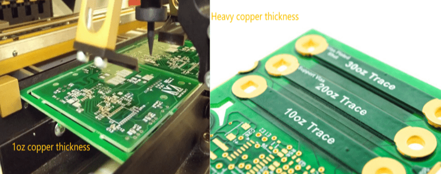
A narrow trace in heavy copper is exposed to lateral attack from both sides. Even modest undercut can remove a meaningful percentage of its designed width. What might be manageable in 1 oz copper becomes much more difficult in 3 oz, 4 oz, or higher copper weights.
This is why heavy copper circuits often require larger minimum trace widths, especially on outer layers that are formed through subtractive etching.
Narrow Spaces Are Harder to Etch Cleanly
Tight spacing also creates difficulty. When gaps are narrow and copper is thick, it becomes harder for the etchant to penetrate, react uniformly, and flush away dissolved copper salts or reaction products efficiently. The result can be incomplete copper removal, localized residue, or poor dimensional consistency along the gap.
The issue is not only whether the space opens, but whether it opens cleanly and repeatably across the full panel.
Etching Uniformity Is More Difficult to Control
Uniformity is another major challenge in heavy copper production.
Even if the nominal copper weight is specified correctly, actual copper thickness is never perfectly identical at every location. Small variation in starting copper, plating distribution, panel pattern density, and local fluid dynamics can all influence how quickly different areas etch.
On a heavy copper panel, those differences matter more because the process window is tighter. Slight differences that might be absorbed in standard copper processing can become visible as measurable variation in trace width, copper residue, or edge definition.
Pattern Density Affects Local Etch Behavior
Dense circuit areas and large open copper areas do not etch in exactly the same way. Local loading changes chemical consumption and flow behavior. A panel with mixed pattern density may show different etch results in different zones unless process balancing is handled carefully.
This is one reason panel uniformity and production engineering matter so much in heavy copper work. Good manufacturability is not only about the single feature, but also about how the entire panel behaves during processing.
Copper Thickness Consistency Matters More
When copper thickness varies, so does required etch time. If one area begins slightly thicker than another, the thinner area may become over-etched by the time the thicker area clears. On heavy copper boards, that gap becomes more significant.
This is why copper thickness consistency, plating distribution, and upstream process stability are closely tied to final etching performance.
Pattern Accuracy and Line Edge Quality Are Harder to Maintain
Pattern accuracy in heavy copper is influenced not only by artwork definition, but by how the copper profile evolves during etching.
Line Edges Tend to Be Less Clean
Heavy copper traces are more prone to irregular line edges, especially when the process approaches its limits. Instead of smooth, consistent conductor edges, the finished pattern may show roughness, waviness, or localized variation.
Uneven line edges can affect electrical consistency, solder mask registration margins, and visual inspection standards. In power electronics, they may also create local field concentration concerns in some designs, depending on voltage and geometry.
Dimensional Deviation Becomes More Likely
As undercut, local etch rate variation, and copper thickness variation accumulate, dimensional deviation becomes harder to avoid. Actual trace width, clearance, pad dimensions, and copper thieving balance can all be affected.
For projects with tight impedance constraints, compact routing, or mechanically constrained landing patterns, this matters well beyond appearance. Dimensional deviation at the etching stage can influence several later manufacturing steps and final product behavior.
Residual Copper Risk Increases
Residual copper is another recurring issue in heavy copper etching, particularly in narrow clearances or difficult-to-clear regions.
If unwanted copper is not fully removed, the result may be partial bridging, conductive residue, or localized copper islands that should not remain. Even if the defect is not immediately catastrophic, it may reduce insulation margin or become a latent reliability concern under temperature cycling, contamination, or voltage stress.
Heavy copper makes this harder because the etchant must remove a larger copper volume while still preserving the intended pattern. The closer the design is to the process limit, the more carefully this balance must be managed.
Practical Project Impact
The etching difficulty of heavy copper boards is not an isolated shop-floor issue. It affects the whole project.
Design Flexibility Becomes More Limited
Heavy copper often forces wider traces, larger spacing, and more conservative routing rules. That may increase board size, reduce routing density, or push the design toward additional layers or alternative copper strategies.
In some cases, the electrical requirement suggests heavy copper, but the layout density suggests otherwise. Resolving that conflict is part of real DFM work.
Yield Pressure Increases
Because the process window is narrower, heavy copper boards are generally more sensitive to variation. Width loss, spacing defects, uneven etching, or residue can have a direct effect on usable yield.
This does not mean heavy copper products are inherently unstable. It means they require stronger process discipline and better fit between design intent and manufacturing capability.
Cost and Lead Time Tend to Increase
Heavy copper boards usually involve more process control effort, more front-end review, and sometimes more iteration between design and manufacturing. Conservative panelization, compensation work, and tighter inspection attention all add practical cost.
Lead time can also be affected, especially when the design pushes close to the limits of trace/space capability for the selected copper weight.
Downstream Fabrication and Assembly Can Be Affected
Etching quality influences more than conductor appearance.
If trace dimensions shift too much, solder mask registration margin may become tighter. If pad geometry changes, assembly performance may be affected. Uneven copper profiles can also influence lamination behavior, surface planarity, and in some cases thermal balance during assembly.
For plated structures, heavy copper geometry can also interact with drilling, plating, and subsequent process uniformity in ways that are less forgiving than standard copper builds.
Reliability Can Be Affected Over Time
Long-term reliability is influenced by whether the actual finished geometry matches what the design intended.
When conductors become narrower than expected, current density rises. When clearances are smaller than intended, insulation margin decreases. When copper residue remains, latent electrical risk increases. When line edges are irregular, localized stress concentration may become more likely in demanding environments.
For power conversion, automotive electronics, industrial controls, and other high-current applications, these details are not secondary. They are part of whether the product remains stable in real operating conditions.
How Manufacturers Typically Address These Challenges
Heavy copper etching cannot be treated as a single-step problem. In practice, manufacturers improve results by controlling the entire pattern formation strategy.
Design Rule Control and Early DFM Review
The first step is often to align copper weight with realistic trace width and spacing capability. If the geometry is too aggressive for the selected copper thickness, the design may need to be adjusted before production begins.
This is where DFM review is essential. It is better to identify an unstable combination of copper thickness and fine geometry at the engineering stage than to discover it later through low yield or inconsistent results.
Etching Compensation
Manufacturers commonly apply etching compensation in the artwork or process planning stage. The principle is straightforward: expected lateral copper loss is considered in advance so the starting pattern can be adjusted to better match the target finished dimensions.
This is not a universal fixed value. Compensation depends on copper thickness, line geometry, process capability, and board structure. The main point is that heavy copper patterns often require more deliberate dimensional compensation than standard boards.
Pattern Plating Where Appropriate
Pattern plating can help reduce the amount of copper that must later be etched away in some process flows. Instead of starting with a very thick copper layer everywhere and subtracting large amounts from open areas, manufacturers may build copper selectively in required circuit areas.
The exact approach depends on the product structure, but the general advantage is that it can reduce etch burden and improve control compared with purely subtractive removal of very thick copper across the entire surface.
Tight Control of Copper Thickness Consistency
Since etching results depend strongly on copper thickness, manufacturers try to control starting copper and plating uniformity as tightly as possible. Better thickness consistency gives a better chance of keeping the etching result consistent across the panel.
This is also why panel balancing, pattern distribution, and upstream process stability matter. Etching performance is linked to the quality of what enters the etching stage.
Panel Uniformity and Process Stability
Heavy copper boards benefit from panel designs and production planning that reduce local extremes in pattern density and process loading. More uniform panel behavior makes etching easier to control.
In practical terms, this may involve panel balancing strategies, process-oriented layout review, and tighter attention to how copper distribution affects production consistency.
Process Window Management
Manufacturers also focus on keeping the process within a stable operating window rather than pushing for the narrowest possible geometry at any cost.
That means controlling chemistry condition, dwell consistency, resist performance, and inspection feedback so the etching process stays repeatable. The objective is not simply to pass one build, but to maintain consistent results over repeated production.
Conclusion
Heavy copper PCB etching is more difficult because the process becomes much less forgiving as copper thickness increases. The main issue is not only the larger copper volume, but the combined effect of deeper etching, greater undercut tendency, reduced line and spacing capability, harder-to-control uniformity, and tighter dimensional tolerances.
That is why the real question in heavy copper PCB manufacturing is not just whether a board can be produced. The more important question is whether the conductor geometry, clearance, and etching result can be controlled consistently from panel to panel and lot to lot.
For heavy copper projects, good manufacturing outcomes depend on that control. Current capacity may be the headline requirement, but etching discipline is often what determines whether the board is actually practical to build, assemble, and rely on in the field.